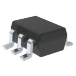
Description of SN74LVC1T45DCKR
This single-bit noninverting bus transceiver makes use of two independent, programmable power rails. The A port’s purpose is to monitor VCCA. Any supply voltage between 1.65 V and 5.5 V is accepted by VCCA. VCCB tracking is intended for the B port.
Any source voltage between 1.65 V and 5.5 V is accepted by VCCB. This enables universal low-voltage bidirectional translation between any of the voltage nodes of 1.8 V, 2.5 V, 3.3 V, and 5 V.
Asynchronous connection between two data buses is supported by the SN74LVC1T45DCKR. Either the B-port outputs or the A-port outputs are activated depending on the direction-control (DIR) input’s logic levels.
When both the B-port outputs and the A-port outputs are active, the device transfers data from the A bus to the B bus and from the B bus to the A bus. A logic HIGH or LOW level must be applied to the input circuitry on both the A and B ports in order to prevent excessive ICC and ICCZ.
The DIR input of the SN74LVC1T45DCKR is intended to be powered by VCCA. This device meets the requirements for Ioff applications involving partial power reduction.
When a device is turned off, the Ioff circuitry turns off the outputs to stop potentially harmful current backflow through the device. The VCC isolation feature is built so that both ports are in the high-impedance condition if either VCC input is at GND.
A significant development in IC packaging ideas is the NanoFree package technology, which uses the die as the package.







Reviews
There are no reviews yet.