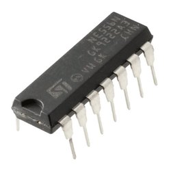
NE555 Timer IC DIP-8 Package
The NE555 IC devices are precision timing circuits capable of producing accurate time delays or oscillation. In the time delay or monostable mode of operation, the timed interval is controlled by a single external resistor and capacitor network. In the a stable mode of operation, the frequency and duty cycle can be controlled independently with two external resistors and a single external capacitor. The threshold and trigger levels normally are two-thirds and one-third, respectively, of VCC. These levels can be altered by use of the control-voltage terminal. When the trigger input falls below the trigger level, the flip-flop is set, and the output goes high. If the trigger input is above the trigger level and the threshold input is above the threshold level, the flip-flop is reset and the output is low. The reset (RESET) input can override all other inputs and can be used to initiate a new timing cycle. When RESET goes low, the flip-flop is reset, and the output goes low. When the output is low, a low impedance path is provided between discharge (DISCH) and ground. The output circuit is capable of sinking or sourcing current up to 200 mA. Operation is specified for supplies of 5V to 15V. With a 5-V supply, output levels are compatible with TTL inputs.
NE556 IC – Dual Timer IC
NE556 IC devices provide two independent timing circuits of the NE555 ?type in each package. These circuits can be operated in the a stable or the monostable mode with external resistor-capacitor (RC) timing control. The basic timing provided by the RC time constant can be controlled actively by modulating the bias of the control-voltage input. The threshold (THRES) and trigger (TRIG) levels normally are two-thirds and one-third, respectively, of VCC. These levels can be altered by using the control voltage (CONT) terminal. When the trigger input falls below trigger level, the flip-flop is set and the output goes high. If the trigger input is above the trigger level and the threshold input is above the threshold level, the flip-flop is reset, and the output is low. The reset (RESET) input can override all other inputs and can be used to initiate a new timing cycle. When RESET goes low, the flip-flop is reset and the output goes low. When the output is low, a low-impedance path is provided between the discharge (DISCH) terminal and ground (GND).
NE556 IC Datasheet
NE592D14R2G
The NE592 is a monolithic, two-stage, differential output,
wideband video amplifier. It offers fixed gains of 100 and 400
without external components and adjustable gains from 400 to 0 with
one external resistor. The input stage has been designed so that with
the addition of a few external reactive elements between the gain
select terminals, the circuit can function as a high-pass, low-pass, or
band-pass filter. This feature makes the circuit ideal for use as a
video or pulse amplifier in communications, magnetic memories,
display, video recorder systems, and floppy disk head amplifiers.
Now available in an 8-pin version with fixed gain of 400 without
external components and adjustable gain from 400 to 0 with one
external resistor.
Features
? 120 MHz Unity Gain Bandwidth
? Adjustable Gains from 0 to 400
? Adjustable Pass Band
? No Frequency Compensation Required
? Wave Shaping with Minimal External Components
? MIL-STD Processing Available
? These Devices are Pb?Free and are RoHS Compliant
Applications
? Floppy Disk Head Amplifier
? Video Amplifier
? Pulse Amplifier in Communications
? Magnetic Memory
? Video Recorder Systems
NE592D8R2G
The NE592 is a monolithic, two-stage, differential output,
wideband video amplifier. It offers fixed gains of 100 and 400
without external components and adjustable gains from 400 to 0 with
one external resistor. The input stage has been designed so that with
the addition of a few external reactive elements between the gain
select terminals, the circuit can function as a high-pass, low-pass, or
band-pass filter. This feature makes the circuit ideal for use as a
video or pulse amplifier in communications, magnetic memories,
display, video recorder systems, and floppy disk head amplifiers.
Now available in an 8-pin version with fixed gain of 400 without
external components and adjustable gain from 400 to 0 with one
external resistor.
Features
? 120 MHz Unity Gain Bandwidth
? Adjustable Gains from 0 to 400
? Adjustable Pass Band
? No Frequency Compensation Required
? Wave Shaping with Minimal External Components
? MIL-STD Processing Available
? These Devices are Pb?Free and are RoHS Compliant
Applications
? Floppy Disk Head Amplifier
? Video Amplifier
? Pulse Amplifier in Communications
? Magnetic Memory
? Video Recorder Systems

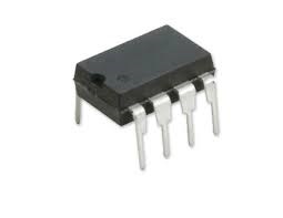
OP07 Ultralow Offset Voltage Op-Amp IC DIP-8
The OP07 has very low input offset voltage (75 ?V maximum for OP07E) that is obtained by trimming at the wafer stage. These low offset voltages generally eliminate any need for external nulling. The OP07 also features low input bias current (?4 nA for the OP07E) and high open-loop gain (200 V/mV for the OP07E). The low offset and high open-loop gain make the OP07 particularly useful for high gain instrumentation applications.
OP177 Ultra-Precision Operational Amplifier IC DIP-8
The OP177 features one of the highest precision performance of any operational amplifier currently available. Offset voltage of the OP177 is only 25 ?V maximum at room temperature. The ultralow VOS of the OP177 combines with the exceptional offset voltage drift (TCVOS) of 0.3 ?V/?C maximum to eliminate the need for external VOS adjustment and increases system accuracy over temperature. The OP177 open-loop gain of 12 V/?V is maintained over the full ?10 V output range. CMRR of 130 dB minimum, PSRR of 120 dB minimum, and maximum supply current of 2 mA are just a few examples of the excellent performance of this operational amplifier. The combination of outstanding specifications of the OP177 ensures accurate performance in high closed-loop gain applications.

PC817X3NIP1B
PC817XxNSZ1B Series contains an IRED optically
coupled to a phototransistor.
It is packaged in a 4-pin DIP.
Input-output isolation voltage(rms) is 5kV.
Collector-emitter voltage is 80V.
CTR is 50% to 400% (at IF=5mA,VCE=5V,Ta=25?)
? Features
1.4-pin DIP package
2. Double transfer mold package
(Ideal for Flow Soldering)
3. High isolation voltage between input and output
(Viso (rms) :5kV)
4. High collector-emitter voltage(VCEO :80V)
5. Current transfer ratio
(CTR : MIN. 50% at IF=5 mA, VCE=5V ,Ta=25?)
6. RoHS directive compliant
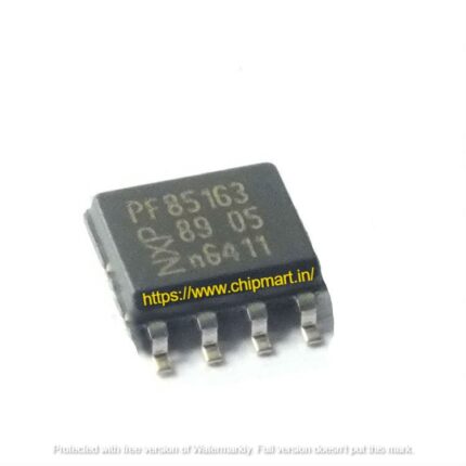
PCF85163D
Nearly any Liquid Crystal Display (LCD)1 with modest multiplex rates may be interfaced with the PCF85162 peripheral device. Any static or multiplexed LCD with up to four backplanes and up to 32 segments can have its driving signals generated by this device. For bigger LCD applications, it is simply cascaded. The two-line bidirectional I2 C-bus is used by the PCF85162 for communication with the majority of microcontrollers. A display RAM with auto-incremented addressing, hardware sub addressing, and display memory switching (static and duplex drive modes) all reduce communication overheads.
Features
LCD controller and driver on a single chip
Selectable display bias configuration: static, 12, or 13; Internal LCD bias generation with voltage-follower buffers; Selectable backplane drive configuration: static, 2, 3, or 4 backplane multiplexing; 32 segment drives:
Up to 8 14-segment alphanumeric characters, up to 16 7-segment numeric characters, and up to 128 components of any image
For storing display data, use 32 bits of RAM.
Flexible flashing modes; switching between display memory banks in static and duplex driving modes; and independent supply for LCD and logic voltage
Broad power supply range: 1.8 to 5.5 volts

PM8909