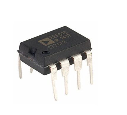
REF01 IC – 10V Precision Voltage Reference IC
The REF01 is industry-standard precision voltage references. The stable 10V output of the REF01 can be adjusted over a ?6% range with minimal effect on temperature stability. The 10V REF01 has a single-supply operation over an input voltage range of 13V to 33V. The devices offer a low-current drain of 1mA.

REF02 IC – 5V Precision Voltage Reference IC
The REF02 are industry-standard precision voltage references. The 5V output REF02 can also be adjusted over a ?6% range. The 5V REF02 has a single-supply operation over an input voltage range of 7V to 33V. Both devices offer a low-current drain of 1mA. The REF02 also provides a TEMP pin whose output voltage varies linearly with temperature, making this device suitable for a wide variety of temperature-sensing and control applications. For new designs, refer to the MAX6035 or MAX6143 data sheets.

REF03 IC – 2.5V Precision Voltage Reference IC
The REF03 precision voltage reference provides a stable 2.5 V output, with minimal change for variations in supply voltage, ambient temperature, or loading conditions. Single-supply operation over an input voltage range of 4.5 V to 33 V with a current drain of 1 mA and good temperature stability is achieved using an improved band gap design. Primarily targeted at price sensitive applications, the REF03 is available in plastic mini DIPs and surface-mount small outline plastic packages. For improved performance or ?40?C to 125?C operation, see the ADR03 data sheet.
SG3524 Regulating Pulse Width Modulator IC DIP-16 Package
SG3524 incorporate all the functions required in the construction of a regulating power supply, inverter, or switching regulator on a single chip. It can be used as the control element for high-power-output applications.SG3524 was designed for switching regulators of either polarity, transformer-coupled dc-to-dc converters, transformerless voltage doublers, and polarity-converter applications employing fixed-frequency, pulse-width modulation (PWM) techniques.

SG3525 Pulse Width Modulation Controller IC DIP-16 Package


SGTL5000XNLA3
Features of SGTL5000XNLA3
Analog inputs
? Stereo LINEIN - External analogue input support
? Stereo LINEIN - Low power codec bypass
? MIC bias was offered
? Adjustable MIC gain
? ADC: -73 dB THD+N (VDDA = 1.8 V) and 85 dB SNR (-60 dB input).
Analog outputs
? Cap less design for HP output
? HP Output: 62.5 mW peak, sine wave @ 1.02 kHz, 16-ohm load at 3.3 V
? HP Output: -80 dB THD+N (VDDA = 1.8 V, 16 load, DAC to headphone) and 100 dB SNR (-60 dB input).
? LINEOUT: -85 dB THD+N (VDDIO = 3.3 V) and 100 dB SNR (-60 dB input).
I/O in digital form of SGTL5000XNLA3
? I2S port for Application Processor Integrated Digital Processing route
? Graphic equaliser clocking/control, NXP surround, NXP bass, and tone control
? PLL provides for the input of system clocks ranging from 8.0 MHz to 27 MHz; standard audio clocks are derived from PLL.
Power Sources of SGTL5000XNLA3
? Created to function between 1.62 and 3.6 volts
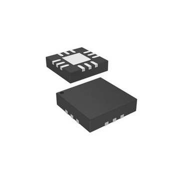
SKY13323-378LF
Features of SKY13323-378LF
- Control of positive voltage (0 and 1.8 V to 0 and 5.0 V)
- The frequency range for broadband is 0.1-3.0 GHz.
- Very low insertion loss, typically 0.35 dB at 3 GHz
- High isolation, typical 27 dB @ 3 GHz
- P1dB = +27 dBm, excellent linearity performance
- MLPD (6-pin, 1 x 1 mm, MSL1, 260 ?C per JEDEC J-STD-020) ultra-compact packaging
- 802.11 b/g WLAN networks
- Wi-Fi repeaters
- ISM-band radios
- Systems for low-power transmission and reception

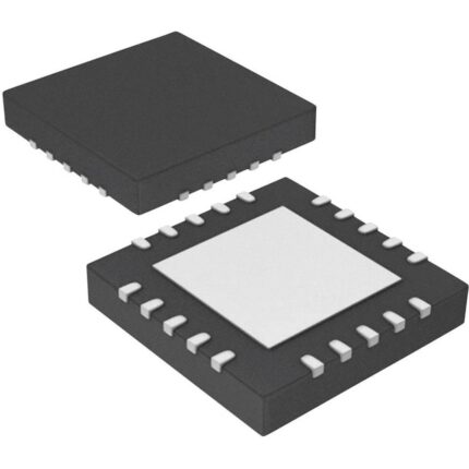
SKY13374-397LF
Features of SKY13374-397LF?
- The frequency range for broadband is 300 kHz to 6.0 GHz.
- Low insertion loss at 1 GHz and 6 GHz: 0.35 dB and 0.8 dB, respectively
- There is no need for external DC blocking capacitors.
- 1.65 to 3.0 V (VCTRL), 2.5 to 4.8 V are examples of positive low control voltages (VBATT)
- QFN (12-pin, 2 x 2 mm) small packaging (MSL1, 260 C per JEDEC J-STD-020)
- Wireless LANs with dual bands (802.11 a/b/g/n)
- Switching between diversity antennas
- WCDMA mobile phones and data cards
- SPDT switch configuration
- Frequency Minimum: 300 kHz
- 6 GHz maximum frequency
- Loss of Insertion: 0.8 dB
- Type of Off Isolation: 2 dB
- 40 C for the minimum operating temperature
- 85 C is the maximum operating temperature.
- SMD/SMT mounting style
- Technology: Si
- Packaging: Reel/ Cut Tape


SN74LVC1T45DCKR
Features of SN74LVC1T45DCKR
? ESD protection is greater than JESD 22 and includes the following models: 2000-V Human-Body Model (A114-A), 200-V Machine Model (A115-A), and 1000-V Charged-Device Model (C101)
? Discreetly accessible in the Texas Instruments NanoFreeTM packaging
? Each port may function throughout the whole 1.65-V to 5.5-V powersupply range thanks to the fully customizable dual-rail design.
? VCC isolation feature: both ports are in the high-impedance condition if either VCC input is at GND.
? Reference to VCCA in the DIR input circuit
? Low power usage, maximum 4-A ICC
? 3.3 V, 24-mA output drive
? Ioff permits operating in partial power-down mode
? The highest data rates are 420 Mbps (3.3-V to 5-V translation)
- 210 Mbps (convert to 3.3 V) (translate to 3.3 V)
- 140 Mbps (convert to 2.5 V) (translate to 2.5 V)
- 75 Mbps (convert to 1.8 V) (translate to 1.8 V)
? Class II JESD 78 latch-up performance exceeds 100 mA
Applications of SN74LVC1T45DCKR
? Personal electronic
? Industrial
? Enterprise
? Telecom


SN74LVC2G241YZPR
Characteristics of the SN74LVC2G241YZPR
- Texas Instruments offers it.
- Packaged in NanoFreeTM
- Supports Operation at 5-V VCC
- Voltage Acceptance to 5.5 V for Inputs
- 4.1 ns maximum tpd at 3.3 V
- Low Power Consumption, ICC at most 10-A
- 3.3 V, 24-mA Output Drive
- At VCC = 3.3 V, TA = 25?C, the typical VOLP (Output Ground Bounce) is 0.8 V. Standard VOHV (Output VOH Undershoot)
- VCC = 3.3 V, TA = 25?C, >2 V
- Live Insertion, Partial-Power-Down Mode, and Back-Drive Protection are supported by Ioff.
- Can Translate Inputs From a Max of 5.5 V Down to the VCC Level When Used as a Down Translator
- Performance of the Latch-Up Exceeds 100 mA Per JESD 78, Class II
- JESD 22 Exceeds ESD Protection
- A/V Receivers
- Home theatre systems with Blu-ray players
- DVD players and recorders
- Desktop or laptop computers
- Internet or digital radio players
- Digital cameras with video (DVC)
- Integrated PCs
- Personal Navigation Systems (GPS)
- Devices for mobile internet
- ?Front-ends for network projectors
- Media Players Portables
- Pro audio mixers


