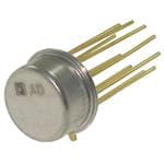
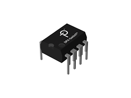
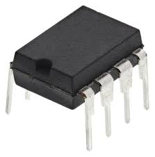
AD536AJH
The AD536A is a complete monolithic integrated circuit that performs the true RMS-to-dc conversion. It offers performance comparable to or superior to that of hybrid or modular units costing much more. The AD536A directly computes the true RMS value of any complex input waveform containing ac and dc components.
Mfr. No: AD536AJH
Mfr.:Analog Devices
Description: Power Management Specialised - PMIC RMS/DC CONVERTER IC
Datasheet: AD536AJH Datasheet (PDF)
AP7165-SPG-13
Features of AP7165-SPG-13
? 2.2V to 5.5V, a broad input voltage range
? 500mA load with a 300mV very low dropout
? Extremely low quiescent current (IQ): typically 125 A
? Total accuracy is less than 2.5% for line, load, and temperature
? 0.8V to 5.0V adjustable output voltage range
? Extremely quick transient reaction
? A high PSRR.
? Reliable voltage control
? Current restriction and short circuit defence
? Thermal shut-off safeguards
? Stable with output capacitors of any kind up to 4.7 F
? A temperature range of -40 to +85 degrees Celsius.
? "Green" molding compound is available in U-DFN3030-10 and SO-8EP (No Br, Sb)
? RoHS Compliant and Lead Free Finish
Application of AP7165-SPG-13
- Servers and laptops
- Smart phone and PDA
- MP3/MP4
- Bluetooth headset
- Low and medium power applications
- FPGA and DSP core or I/O power
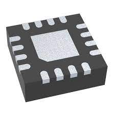
BQ24230RGT
Features of BQ24230
- Up to 500 mA of charge current is supported, and a current monitoring output is provided (ISET)
- For wall adapters, programmable input current limit of up to 500 mA
- Termination Current With Programmability (bq24232)
- Pre-charge and fast-charge safety timers that are programmable
- Short-Circuit, Thermal, and Reverse Current Protection
- Input NTC Thermistor
- Exclusive Start-Up Sequence Controls Inrush Current
- Charged/Done Status Indication, Good Power
- 16-Lead 3 mm x 3 mm Small QFN Package
- With Overvoltage Protection and a 28-V Input Rating
- Function of Integrated Dynamic Power-Path Management (DPPM) Powers the System and Charges the Battery Separately and Concurrently
- ? USB Charger Fully Compliant - Selectable Maximum Input Current of 100 mA and 500 mA - The USB-IF standard is ensured by the 100-mA maximum current limit. - Protection Against Subpar USB Sources using Input-based Dynamic Power Management (VIN- DPM)
- Bluetooth? Devices
- Low-Power Handheld Devices
BQ25100YFP
Features of BQ25100YFP
- Adjustable thresholds for termination and pre-charge
- Dynamic input voltage power management
- ISET short detection and OUT short-circuit prevention
- 10 hour fixed safety timer
- 1% accuracy in charge voltage
- 10% accuracy in charge current
- Green products without Sb or Br
- Recharge - 1% Accuracy in Charge Voltage - 10 percent charge current accuracy - Supports 10 mA to 250 mA charge current applications. - Supports a 1-mA charge termination current minimum -Maximum 75 nA Ultra Low Battery Output Leakage Current
- Adjustable Pre-charge and Termination Threshold
- 4.35V with bq25100H/01H and 4.30V with bq25100A for high voltage chemistry support
- Fitness Equipment
- A smart watch
- Headsets with Bluetooth?
- Low-Power Portable Electronics
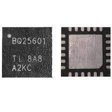
BQ25601RTW
Features of BQ25601RTW
- High-efficiency, 1.5 MHz, synchronous switch-mode buck charger - 92% charge efficiency at 2 A from 5 V input - Optimized for USB voltage input (5 V)
- Supports USB OTG - Boost converter with up to 1.2 A output - 92% boost efficiency at 1 A output - Accurate constant current (CC) limit - Soft-start up to 500 ?F capacitive load - Output short-circuit protection
- Single input to support USB input and high voltage adapters - Support 3.9 V to 13.5 V input voltage range with 20 V absolute maximum input voltage rating - Maximum power tracking by input voltage limit up to 4.6 V (VINDPM) - VINDPM threshold automatically tracks battery voltage - Auto detect USB SDP, DCP and non-standard adapters
- 200 nS fast turn-off of optional external OVPFET standing input voltage up to 40?V
- High battery discharge efficiency with 19.5 m? battery discharge MOSFET
- High integration includes all MOSFETs, current sensing, and loop compensation
- 58 ?A low battery leakage current with system voltage standby
- EPOS, portable speakers, e-cigarettes
- Portable internet devices and accessories
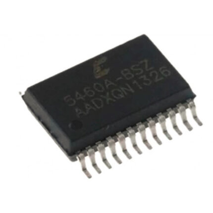
CS5460A-BS IC
CS5460A-BS IC ? (SMD SSOP-24 Package) ? Single Phase Bi-Directional Power/Energy IC
CS5460A-BS IC is a highly integrated power measurement solution that combines two Analog-to-digital Converters (ADCs), high-speed power calculation functions, and a serial interface on a single chip. It is designed to accurately measure and calculate: Real (True) Energy, Instantaneous Power, IRMS, and VRMS for single phase 2- or 3-wire power metering applications. The CS5460A interfaces to a low-cost shunt resistor or transformer to measure current, and to a resistive divider or potential transformer to measure voltage. The CS5460A features a bi-directional serial interface for communication with a microcontroller and a pulse output engine for which the average pulse frequency is proportional to the real power. The CS5460A has on-chip functionality to facilitate AC or DC system-level calibration.CS5460A-BSZ
The CS5460A is a single-chip Delta-Sigma analog/digital converter (ADC) that integrates two Delta-Sigma ADCs, high-speed power calculation capabilities, and a serial interface. It is intended to precisely measure and compute energy, immediate power, IRMS, and VRMS for single-phase, two-wire, or three-wire power metering applications.
To measure current, the CS5460A attaches to a low-cost shunt resistor or transformer, and to a resistant divider or potential transformer to monitor voltage. It has a bidirectional serial interface for communicating with a microcontroller, as well as a configurable frequency output that is proportionate to energy. The CS5460A includes on-chip capabilities for AC or DC framework calibration.
The "Auto-Boot" functionality enables the CS5460A to operate independently and to initialise itself upon system power-up. The CS5460A reads dataset and begins giving??directives from an external EEPROM during Auto-Boot mode. In this mode, the CS5460A may operate without the need of a microprocessor, making it ideal for reduced cost??measuring purposes.
DPA422PN
The DPA-Switch? IC family is a highly integrated solution for
DC-DC conversion applications with 16-75 VDC input.
DPA-Switch uses the same proven topology as TOPSwitch?,
cost effectively integrating a power MOSFET, PWM control, fault
protection and other control circuitry onto a single CMOS chip.
High performance features are enabled with three user
configurable pins. Hysteretic thermal shutdown is also provided.
In addition, all critical parameters (i.e. current limit, frequency,
PWM gain) have tight temperature and absolute tolerance, to
simplify design and reduce system cost.
DPA423PN
The DPA-Switch? IC family is a highly integrated solution for
DC-DC conversion applications with 16-75 VDC input.
DPA-Switch uses the same proven topology as TOPSwitch?,
cost effectively integrating a power MOSFET, PWM control, fault
protection and other control circuitry onto a single CMOS chip.
High performance features are enabled with three user
configurable pins. Hysteretic thermal shutdown is also provided.
In addition, all critical parameters (i.e. current limit, frequency,
PWM gain) have tight temperature and absolute tolerance, to
simplify design and reduce system cost.
DPA425PN
The DPA-Switch? IC family is a highly integrated solution for
DC-DC conversion applications with 16-75 VDC input.
DPA-Switch uses the same proven topology as TOPSwitch?,
cost effectively integrating a power MOSFET, PWM control, fault
protection and other control circuitry onto a single CMOS chip.
High performance features are enabled with three user
configurable pins. Hysteretic thermal shutdown is also provided.
In addition, all critical parameters (i.e. current limit, frequency,
PWM gain) have tight temperature and absolute tolerance, to
simplify design and reduce system cost.
LKN614PN
LM2931CMX/NOPB
Features of LM2931CMX/NOPB
? Extremely Minimal Quiescent Current
? An output current greater than 100 mA
? Less than 0.6V in input-output differential
? Battery reverse protection
? 60V Load Dump Security
? Reverse Transient Protection at 50 volts
? Protection against Short Circuits
? Protection from Internal Thermal Overload
? Available in SOIC-8, TO-220, TO-92, or TO-263 packages
? Adjustable using TTL Compatible Switches are readily available.

