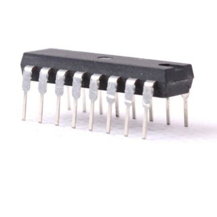
SN75175N
The SN65175 and SN75175 are monolithic quadruple differential line receivers with 3-state outputs. They are
designed to meet the requirements of ANSI Standards EIA/TIA-422-B, RS-423-B, and RS-485, and several ITU
recommendations. These standards are for balanced multipoint bus transmission at rates up to 10 megabits
per second. Each of the two pairs of receivers has a common active-high enable.
SN75179BP
The SN75179B is a differential driver and receiver pair designed for balanced transmission-line applications
and meets TIA/EIA-422-B, TIA/EIA-485-A, and ITU Recommendation V.11. It is designed to improve the
performance of full-duplex data communications over long bus lines.
The SN75179B driver output provides limiting for both positive and negative currents. The receiver features high
input impedance, input hysteresis for increased noise immunity, and input sensitivity of ?200 mV over a
common-mode input voltage range of ?7 V to 12 V. The driver provides thermal shutdown for protection from
line fault conditions. Thermal shutdown is designed to occur at a junction temperature of approximately 150?C.
The SN75179B is designed to drive current loads of up to 60 mA maximum.
The SN75179B is characterized for operation from 0?C to 70?C.
SN75451B
The SN5545xB and SN7545xB devices are dualperipheral drivers designed for use in systems that
employ TTL logic. This family is functionally
interchangeable with and replaces the SN75450
family and the SN75450A family devices
manufactured previously. The speed of the devices is
equal to that of the SN75450 family, and the parts are
designed to ensure freedom from latch-up. Diodeclamped inputs simplify circuit design.
SN75453BP
The SN5545xB and SN7545xB devices are dualperipheral drivers designed for use in systems that
employ TTL logic. This family is functionally
interchangeable with and replaces the SN75450
family and the SN75450A family devices
manufactured previously. The speed of the devices is
equal to that of the SN75450 family, and the parts are
designed to ensure freedom from latch-up. Diodeclamped inputs simplify circuit design
SN75468N
The SN75468 and SN75469 are high-voltage, high1? 500-mA Rated Collector Current (Single Output)
current Darlington transistor arrays. Each consists of
? High-Voltage Output 100 V seven NPN Darlington pairs that feature high-voltage
? Output Clamp Diodes outputs with common-cathode clamp diodes for
? Inputs Compatible With Various Types of Logic switching inductive loads. The collector-current rating
of each Darlington pair is 500 mA. The Darlington
? Relay Driver Applications pairs may be paralleled for higher current capability.
? Higher-Voltage Versions of ULN2003A and Applications include relay drivers, hammer drivers,
ULN2004A, for Commercial Temperature range lamp drivers, display drivers (LED and gas
discharge), line drivers, and logic buffers
SN75477P
? Characterized for Use to 300 mA
? No Output Latch-Up at 55 V (After
Conducting 300 mA)
? High-Voltage Outputs (100 V Typ)
? Output Clamp Diodes for Transient
Suppression (300 mA, 70 V)
? TTL- or MOS-Compatible Diode-Clamped
Inputs
? pnp Transistor Inputs Reduce Input Current
? Standard Supply Voltage
? Suitable for Hammer-Driver Applications
? Plastic DIP (P) With Copper-Lead Frame
Provides Cooler Operation and Improved
Reliability
SN75ALS180N
SN75ALS197N
The SN75ALSI97 is a monolithic, quadruple line receiver with 3-state outputs designed using advanced,
low-power, Schottky technology. This technology provides combined improvements in bar design, tooling
production, and wafer fabrication. This, in turn, provides significantly lower power requirements and permits
much higher data throughput than other designs. The device meets the specifications of ITU Recommendations
V.10, V.11, X.26, and X.27. It features 3-state outputs that permit direct connection to a bus-organized system
with a fail-safe design that ensures the outputs will always be high if the inputs are open.
SN75C188N
The SN75C188 is a monolithic, low-power, quadruple line driver that interfaces data terminal equipment with
data communications equipment. This device is designed to conform to ANSI Standard EIA/TIA-232-E.
An external diode in series with each supply-voltage terminal is needed to protect the SN75C188 under certain
fault conditions to comply with EIA/TIA-232-E.
The SN75C188 is characterized for operation from 0?C to 70?C.


