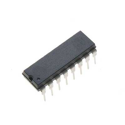
TNY266G
TinySwitch?-II integrates a 700 V power MOSFET, oscillator,
high voltage switched current source, current limit and thermal
shutdown circuitry onto a monolithic device. The start-up and
operating power are derived directly from the voltage on the
DRAIN pin, eliminating the need for a bias winding and associated
circuitry. In addition, the TinySwitch-II devices incorporate
auto-restart, line undervoltage sense, and frequency jittering. An
innovative design minimizes audio frequency components in the
simple ON/OFF control scheme to practically eliminate audible
noise with standard taped/varnished transformer construction.
PI-2684-061815
Wide-Range
High-Voltage
DC Input D
S
EN/UV
BP
-
-
DC
Output
TinySwitch-II
Optional
UV Resistor
The fully integrated auto-restart circuit safely limits output power
during fault conditions such as output short circuit or open loop,
reducing component count and secondary feedback circuitry
cost. An optional line sense resistor externally programs a line
undervoltage threshold, which eliminates power down glitches
caused by the slow discharge of input storage capacitors present
in applications such as standby supplies. The operating
frequency of 132 kHz is jittered to significantly reduce both the
quasi-peak and average EMI, minimizing filtering cost.
TNY267PN
TinySwitch?-II integrates a 700 V power MOSFET, oscillator,
high voltage switched current source, current limit and thermal
shutdown circuitry onto a monolithic device. The start-up and
operating power are derived directly from the voltage on the
DRAIN pin, eliminating the need for a bias winding and associated
circuitry. In addition, the TinySwitch-II devices incorporate
auto-restart, line undervoltage sense, and frequency jittering. An
innovative design minimizes audio frequency components in the
simple ON/OFF control scheme to practically eliminate audible
noise with standard taped/varnished transformer construction.
TPC8089-H
This N-Channel MOSFET employs cutting-edge trench technology to achieve high RDS(on) while maintaining a low gate charge. It can be applied to a wide range of situations.
Features?
1)VDS=40V,ID=6.7A,RDS(ON)<32m?@VGS=10V
2)Low gate charge.
3)Green device available.
4)Advanced high cell denity trench technology for ultra R
DS(ON).
5)Excellent package for good heat dissipation
TYN616 – 600V – 16A SCR – Thyristor
U403
The -50V InterFET IFNU401, IFNU402, and
IFNU403 JFET?s are targeted for low noise
differential amplifier designs. Gate leakages are
less than 10pA at room temperatures. The TO-71
package is hermetically sealed and suitable for
military applications. Custom specifications,
matching, and packaging options are available.


