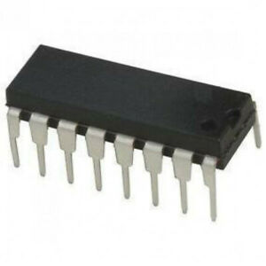
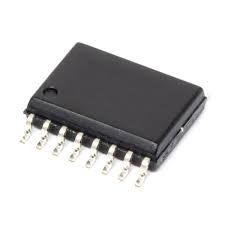
AD847JR
Superior Performance
High Unity Gain BW: 50 MHz
Low Supply Current: 5.3 mA
High Slew Rate: 300 V/ms
Excellent Video Specifications
0.04% Differential Gain (NTSC and PAL)
0.198 Differential Phase (NTSC and PAL)
Drives Any Capacitive Load
Fast Settling Time to 0.1% (10 V Step): 65 ns
Excellent DC Performance
High Open-Loop Gain 5.5 V/mV (RLOAD = 1 kV)
Low Input Offset Voltage: 0.5 mV
Specified for 65 V and 615 V Operation
Available in a Wide Variety of Options
Plastic DIP and SOIC Packages
Cerdip Package
Die Form
MIL-STD-883B Processing
Tape & Reel (EIA-481A Standard)
Dual Version Available: AD827 (8 Lead)
Enhanced Replacement for LM6361
Replacement for HA2544, HA2520/2/5 and EL2020
APPLICATIONS
Video Instrumentation
Imaging Equipment
Copiers, Fax, Scanners, Cameras
High Speed Cable Driver
High Speed DAC and Flash ADC Buffers
AD8551ARM
This family of amplifiers has ultralow offset, drift, and bias
current. The AD8551, AD8552, and AD8554 are single, dual,
and quad amplifiers featuring rail-to-rail input and output swings.
All are guaranteed to operate from 2.7 V to 5 V with a single supply.
The AD8551/AD8552/AD8554 provide the benefits previously
found only in expensive auto-zeroing or chopper-stabilized
amplifiers. Using Analog Devices, Inc. topology, these new
zero-drift amplifiers combine low cost with high accuracy. No
external capacitors are required.
AD8561A
The AD8561 is a single 7 ns comparator with separate input and
output sections. Separate supplies enable the input stage to be
operated from ?5 V dual supplies and 5 V single supplies.
Fast 7 ns propagation delay makes the AD8561 a good choice
for timing circuits and line receivers. Propagation delays for
rising and falling signals are closely matched and track over
temperature. This matched delay makes the AD8561 a good
choice for clock recovery, since the duty cycle of the output will
match the duty cycle of the input.
AD8561ANZ
The AD8561 is a single 7 ns comparator with separate input and
output sections. Separate supplies enable the input stage to be
operated from ?5 V dual supplies and 5 V single supplies.
Fast 7 ns propagation delay makes the AD8561 a good choice
for timing circuits and line receivers. Propagation delays for
rising and falling signals are closely matched and track over
temperature. This matched delay makes the AD8561 a good
choice for clock recovery, since the duty cycle of the output will
match the duty cycle of the input.
The AD8561 has the same pinout as the LT1016, with lower
supply current and a wider common-mode input range, which
includes the negative supply rail.
The AD8561 is specified over the industrial (?40?C to 85?C)
temperature range. The AD8561 is available in the 8-lead
plastic DIP, 8-lead TSSOP, and 8-lead narrow SOIC surfacemount packages.
AD9241AS
The AD9241 is a 1.25 MSPS, single supply, 14-bit analog-todigital converter (ADC). It combines a low cost, high speed
CMOS process and a novel architecture to achieve the resolution
and speed of existing hybrid implementations at a fraction of the
power consumption and cost. It is a complete, monolithic ADC
with an on-chip, high performance, low noise sample-and-hold
amplifier and programmable voltage reference. An external reference can also be chosen to suit the dc accuracy and temperature
drift requirements of the application. The device uses a multistage
differential pipelined architecture with digital output error correction logic to guarantee no missing codes over the full operating
temperature range
ADC0808N
The ADC0808, ADC0809 data acquisition component
2? Easy Interface to All Microprocessors
is a monolithic CMOS device with an 8-bit analog-to-
? Operates Ratiometrically or with 5 VDC or digital converter, 8-channel multiplexer and
Analog Span Adjusted Voltage Reference microprocessor compatible control logic. The 8-bit
? No Zero or Full-Scale Adjust Required A/D converter uses successive approximation as the
conversion technique. The converter features a high ? 8-Channel Multiplexer with Address Logic
impedance chopper stabilized comparator, a 256R
? 0V to VCC Input Range voltage divider with analog switch tree and a
? Outputs meet TTL Voltage Level Specifications successive approximation register. The 8-channel
? ADC0808 Equivalent to MM74C949 multiplexer can directly access any of 8-single-ended
analog signals
ADC0838CIWM
The ADC0831 series are 8-bit successive
Address Logic approximation A/D converters with a serial I/O and
configurable input multiplexers with up to 8 channels. ? Shunt Regulator Allows Operation with High
The serial I/O is configured to comply with the TI Voltage Supplies MICROWIRE serial data exchange standard for easy
? 0V to 5V Input Range with Single 5V Power interface to the COPS family of processors, and can
Supply interface with standard shift registers or ?Ps.
? Remote Operation with Serial Digital Data Link The 2-, 4- or 8-channel multiplexers are software
? TTL/MOS Input/Output Compatible configured for single-ended or differential inputs as
? 0.3 well as channel assignment. in. Standard Width, 8-, 14- or 20-Pin PDIP
Package The differential analog voltage input allows increasing
? 20 Pin PLCC Package (ADC0838-N Only) the common-mode rejection and offsetting the analog
zero input voltage value. In addition, the voltage ? SOIC Package
reference input can be adjusted to allow encoding
any smaller analog voltage span to the full 8 bits of
resolution
ADE7763ARSZ
phase matching between the current and the voltage channels.
The ADE7763 provides a serial interface to read data and a
pulse output frequency (CF) that is proportional to the active
power. Various system calibration features such as channel
offset correction, phase calibration, and power calibration
ensure high accuracy. The part also detects short duration, low
or high voltage variations.
The positive-only accumulation mode gives the option to
accumulate energy only when positive power is detected. An
internal no-load threshold ensures that the part does not exhibit
any creep when there is no load. The zero-crossing output (ZX)
produces a pulse that is synchronized to the zero-crossing point
of the line voltage. This signal is used internally in the line cycle
active and apparent energy accumulation modes, which enables
faster calibration

