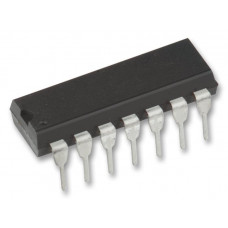
74HC165 8-Bit Parallel In/Serial Out Shift Register IC (74165 IC) DIP-16 Package
₹15.00
The 74HC165 high speed PARALLEL-IN/SERIAL-OUT SHIFT REGISTER utilizes advanced silicon-gate CMOS technology. It has the low power consumption and high noise immunity of standard CMOS integrated circuits, along with the ability to drive 10 LS-TTL loads.
Also included is a gated CLOCK input and a complementary output from the eighth bit. Clocking is accomplished through a 2-input NOR gate permitting one input to be used as a CLOCK INHIBIT function. Holding either of the CLOCK inputs high inhibits clocking, and holding either CLOCK input low with the SHIFT/LOAD input high enables the other CLOCK input. Data transfer occurs on the positive going edge of the clock.
Parallel loading is inhibited as long as the SHIFT/LOAD input is HIGH. When taken LOW, data at the parallel inputs is loaded directly into the register independent of the state of the clock. The 74HC logic family is functionally as well as pin-out compatible with the standard 74LS logic family. All inputs are protected from damage due to static discharge by internal diode clamps to VCC and ground.
Features :-
???Typical propagation delay: 20 ns (clock to Q)
???Wide operating supply voltage range: 2?6V
???Low input current: 1 ?A maximum
???Low quiescent supply current: 80 ?A maximum (74HC Series)
???Fanout of 10 LS-TTL loads
Specifications:-
| Parameter | Specification |
| Supply Voltage (VCC | ? 0.5 to + 7.0V DC |
| Input Voltage (VIN) | ??1.5V to VDD + 1.5V |
| Output Voltage (VOUT) | ?? 0.5 to VCC + 0.5V |
| Clamp Diode Current (IIK, IOK) | ? ?? 20 mA |
| DC Output Current, per pin (IOUT) | ? 25 mA |
| ? ?DC VCC or GND Current, per pin (ICC) | ? 50 mA |
| ?Storage Temperature Range (TSTG) | ? 65?C to + 150?C |
| Power Dissipation (PD) (Note 4) | ?600 mW |
| S.O. Package only | ? 500 mW |
| Lead Temperature (TL) | 260?C |
Related Document:-
 ?74HC165 IC Datasheet
* Product Images are shown for illustrative purposes only and may differ from actual product.


MAECENAS IACULIS
Vestibulum curae torquent diam diam commodo parturient penatibus nunc dui adipiscing convallis bulum parturient suspendisse parturient a.Parturient in parturient scelerisque nibh lectus quam a natoque adipiscing a vestibulum hendrerit et pharetra fames nunc natoque dui.
ADIPISCING CONVALLIS BULUM
- Vestibulum penatibus nunc dui adipiscing convallis bulum parturient suspendisse.
- Abitur parturient praesent lectus quam a natoque adipiscing a vestibulum hendre.
- Diam parturient dictumst parturient scelerisque nibh lectus.
Scelerisque adipiscing bibendum sem vestibulum et in a a a purus lectus faucibus lobortis tincidunt purus lectus nisl class eros.Condimentum a et ullamcorper dictumst mus et tristique elementum nam inceptos hac parturient scelerisque vestibulum amet elit ut volutpat.


