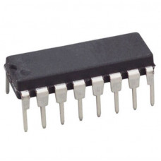
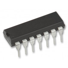
The 74HC595 high speed shift register utilizes advanced silicon-gate CMOS technology. This device possesses the high noise immunity and low power consumption of standard CMOS integrated circuits, as well as the ability to drive 15 LS-TTL loads. This device contains an 8-bit serial-in, parallel-out shift register that feeds an 8-bit D-type storage register. The storage register has 8 3-STATE outputs. Separate clocks are provided for both the shift register and the storage register.
The shift register has a direct-overriding clear, serial input, and serial output (standard) pins for cascading. Both the shift register and storage register use positive-edge triggered clocks. If both clocks are connected together, the shift register state will always be one clock pulse ahead of the storage register. The 74HC logic family is speed, function, and pin-out compatible with the standard 74LS logic family. All inputs are protected from damage due to static discharge by internal diode clamps to VCC and ground.
Features:-
??Low quiescent current: 80 ?A maximum (74HC Series)
??Low input current: 1 ?A maximum
??8-bit serial-in, parallel-out shift register with storage
??Wide operating voltage range: 2V?6V
??Shift register has direct clear
??Guaranteed shift frequency: DC to 30 MHz
Specifications:-
| Parameter | Specification |
| Supply Voltage (VCC | ? 0.5 to + 7.0V |
| Input Voltage (VIN) | ??1.5V to VCC + 1.5V |
| Output Voltage (VOUT) | ?? 0.5 to VCC + 0.5V |
| Clamp Diode Current (IIK, IOK) | ? ?? 20 mA |
| DC Output Current, per pin (IOUT) | ? 35 mA |
| ? ?DC VCC or GND Current, per pin (ICC) | ? 70 mA |
| ?Storage Temperature Range (TSTG) | ? 65?C to + 150?C |
| Power Dissipation (PD) (Note 4) | ?600 mW |
| S.O. Package only | ? 500 mW |
| Lead Temperature (TL) (Soldering 10 seconds) | 260?C |
Related Document:-
 ?74HC595 IC Datasheet
* Product Images are shown for illustrative purposes only and may differ from actual product.