89E516RD2
₹550.00
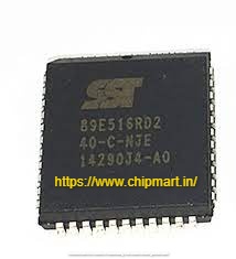
The SST89E5xxRD2 and SST89V5xxRD2 are FlashFlex51 family 8-bit microcontroller devices designed and manufactured using SST’s unique and proprietary Super Flash CMOS semiconductor manufacturing technology. SST’s clients gain significantly from the split-gate device structure and thick-oxide tunnelling injector in terms of cost and reliability. The devices are pin-for-pin compatible with ordinary 8051 microcontroller devices and use the 8051 instruction set. The devices include 16/24/40/72 K Byte of on-chip flash EEPROM programme memory that is divided into two separate programme memory blocks. The primary Block 0 has 8/16/32/64K Bytes of internal programme memory space, whereas the secondary Block 1 has 8K Bytes of internal programme memory space.
The 8-KByte secondary block can be identified to the minimum address point in the 8/16/32/64 K Byte address space, as well as concealed from the programme counter and utilised as an independent EEPROM-like data store. In addition to the on-chip EEPROM programme memory of 16/24/40/72 K Bytes, the devices may address up to 64 K Bytes of external programme memory. In addition to 1024 x 8 bits of on-chip RAM, external RAM of up to 64 K Bytes may be addressed.


MAECENAS IACULIS
Vestibulum curae torquent diam diam commodo parturient penatibus nunc dui adipiscing convallis bulum parturient suspendisse parturient a.Parturient in parturient scelerisque nibh lectus quam a natoque adipiscing a vestibulum hendrerit et pharetra fames nunc natoque dui.
ADIPISCING CONVALLIS BULUM
- Vestibulum penatibus nunc dui adipiscing convallis bulum parturient suspendisse.
- Abitur parturient praesent lectus quam a natoque adipiscing a vestibulum hendre.
- Diam parturient dictumst parturient scelerisque nibh lectus.
Scelerisque adipiscing bibendum sem vestibulum et in a a a purus lectus faucibus lobortis tincidunt purus lectus nisl class eros.Condimentum a et ullamcorper dictumst mus et tristique elementum nam inceptos hac parturient scelerisque vestibulum amet elit ut volutpat.
Related products
24C32 32K bit
25AA320-I/SN
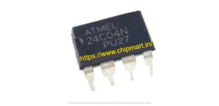
AT24CO4
AT25640B-SSHL-T
HT9200A
M24128-DRDW8TP/K
- Support for all I2C bus modes? 1 MHz/ 400 kHz/ 100 kHz
- Memory bank- An EEPROM with 128 Kbits (16 Kbytes)
- Page Size in Bytes: 64
- In addition Make a locked page.
- Wider range of temperatures and voltages?40 to 105 degrees Celsius; 1.7 to 5.5 volts
- Schmitt trigger inputs are used to filter noise.
- Cycle time for short writes- Byte Write in 4 milliseconds- Page Write in 4 milliseconds
- Express cycling stamina. -4,000,000 Write Cycles at 25 ?C, - 1,2,000,000 Write cycles at 85 ?C & ? 900 k Cycles of writing at 105 ?C
- Data storage- at 105 ?C for more than 50 years., 200 yr at 55 ?C
- ESD Defense (Human Body Model)? 4000 V
- Packing is- Halogen-free and RoHS compliant
- SMD/SMT mounting style
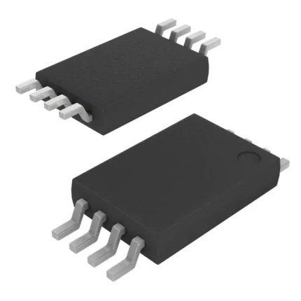
- Case/Package: TSSOP-8
- Interface types: I2C and 2-Wire
- Size of Memory: 128 kbit
- Arrangement: 16 k x 8
- Minimum Supply Voltage: 1.7 V
- Maximum Supply Voltage: 5.5 V
- 40 C for the minimum operating temperature
- 105 C is the maximum operating temperature.
- 1 MHz is the maximum clock frequency.
- Time to Access: 450 ns
- Retention of Data: 200 Years
- Maximum Supply Current: 2 mA
- The M24128-DRD series
- mandatory requirement: AEC-Q100
- Packaging: Cut Tape and Reel
- Maximum Active Read Current: 2 mA
- STMicroelectronics is a brand.
- 2 mA is the operating supply current.
- Voltage Range for Operating Supply: 1.8 to 5.5 V
- Type of Product: EEPROM
M25P40-VMN6TPB
- ?4 Mbit of Flash memory
- ?2.3 V to 3.6 V single supply voltage
- ?SPI bus compatible serial interface
- ?75 MHz clock rate (maximum)
- ?Page Program (up to 256 bytes) in 0.8 ms (typical)
- ?Sector Erase (512 Kbit) in 0.6 s (typical)
- ?Bulk Erase (4 Mbit) in 4.5 s (typical)
- ?Deep Power-down mode 1 ?A (typical)
- ?Hardware Write Protection: protected area size defined by three non-volatile bits (BP0, BP1 and BP2)
- ?Electronic signatures ? JEDEC standard two-byte signature (2013h) ? Unique ID code (UID) with 16 bytes read only, available upon customer request ? RES instruction, one-byte, signature (12h), for backward compatibility
- ?Packages ? RoHS compliant
- ?Automotive grade parts available
- Memory Size -
- Supply Voltage - Min: 2.3 V
- Supply Voltage - Max: 3.6 V
- Active Read Current - Max: 8 mA
- Interface Type: SPI
- Maximum Clock Frequency: 75 MHz
- Organisation: 512 k x 8
- Data Bus Width: 8 bit
- Timing Type: Synchronous
- Minimum Operating Temperature: - 40 C
- Maximum Operating Temperature: + 85 C
- Packaging: Reel / Cut Tape
- Memory Type: NOR
- Product Type: NOR Flash
- Speed: 75 MHz






Reviews
There are no reviews yet.