
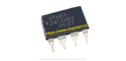
AT24CO2
₹25.00
The 1024/2048/4096/8192/16384 bits of serial electrically erasable and programmable read-only memory (EEPROM) provided by the AT24C01A/02/04/08A/16A are structured as 128/256/512/1024/2048 words of 8 bits each. The gadget is designed with a variety of industrial and business applications in mind, where low-power and low-voltage functioning are crucial. The AT24C01A/02/04/08A/16A is accessible through a Two-wire serial interface and is offered in compact 8-lead PDIP, 8-lead JEDEC SOIC, 8-lead MAP, 5-lead SOT23 (AT24C01A/AT24C02/AT24C04), 8-lead TSSOP, and 8-ball dBGA2 packages. There are other variants of the complete series in 2.7V (2.7V to 5.5V) and 1.8V (1.8V to 5.5V) voltage ranges.
Features
Low and Standard Voltage Operation: 2.7 (VCC = 2.7 to 5.5 V) and 1.8 (VCC = 1.8 to 5.5 V)
?128 x 8, 256 x 8, 512 x 8, 1024 x 8, or 2048 x 8 internal organisation (16K)
Bidirectional Data Transfer Protocol, Schmidt Trigger, Filtered Inputs for Noise Suppression, Two-wire Serial Interface, and Compatibility at 100 kHz (1.8V) and 400 kHz (2.7V, 5V)
8-byte page (1K, 2K), 16-byte page, Write Protect Pin for Hardware Data Protection (4K, 8K, 16K) Writing Styles
?High-reliability? Endurance: 1 Million Write Cycles? Data Retention: 100 Years ?Partial Page Writes Allowed ?Self-timed Write Cycle (5 ms max)
?Automotive Grade and Lead-free/Halogen-free Devices Available
?5-lead SOT23,8-lead TSSOP,8-lead PDIP,8-lead JEDEC SOIC,8-lead MAP, and 8-ball dBGA2 Packages
?Die Sales: Bumped Wafers, Waffle Packs, and Wafer Forms


MAECENAS IACULIS
Vestibulum curae torquent diam diam commodo parturient penatibus nunc dui adipiscing convallis bulum parturient suspendisse parturient a.Parturient in parturient scelerisque nibh lectus quam a natoque adipiscing a vestibulum hendrerit et pharetra fames nunc natoque dui.
ADIPISCING CONVALLIS BULUM
- Vestibulum penatibus nunc dui adipiscing convallis bulum parturient suspendisse.
- Abitur parturient praesent lectus quam a natoque adipiscing a vestibulum hendre.
- Diam parturient dictumst parturient scelerisque nibh lectus.
Scelerisque adipiscing bibendum sem vestibulum et in a a a purus lectus faucibus lobortis tincidunt purus lectus nisl class eros.Condimentum a et ullamcorper dictumst mus et tristique elementum nam inceptos hac parturient scelerisque vestibulum amet elit ut volutpat.
Related products
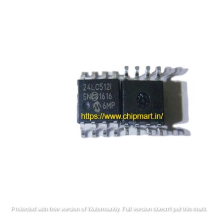
24LC512-I/SN
25AA320-I/SN

AT24C512C-SSHD
AT25640B-SSHL-T

AT89C55WD-24PU – Microchip – 8 Bit MCU, 8051
HT9200A


M25P40-VMN6TPB
- ?4 Mbit of Flash memory
- ?2.3 V to 3.6 V single supply voltage
- ?SPI bus compatible serial interface
- ?75 MHz clock rate (maximum)
- ?Page Program (up to 256 bytes) in 0.8 ms (typical)
- ?Sector Erase (512 Kbit) in 0.6 s (typical)
- ?Bulk Erase (4 Mbit) in 4.5 s (typical)
- ?Deep Power-down mode 1 ?A (typical)
- ?Hardware Write Protection: protected area size defined by three non-volatile bits (BP0, BP1 and BP2)
- ?Electronic signatures ? JEDEC standard two-byte signature (2013h) ? Unique ID code (UID) with 16 bytes read only, available upon customer request ? RES instruction, one-byte, signature (12h), for backward compatibility
- ?Packages ? RoHS compliant
- ?Automotive grade parts available
- Memory Size -
- Supply Voltage - Min: 2.3 V
- Supply Voltage - Max: 3.6 V
- Active Read Current - Max: 8 mA
- Interface Type: SPI
- Maximum Clock Frequency: 75 MHz
- Organisation: 512 k x 8
- Data Bus Width: 8 bit
- Timing Type: Synchronous
- Minimum Operating Temperature: - 40 C
- Maximum Operating Temperature: + 85 C
- Packaging: Reel / Cut Tape
- Memory Type: NOR
- Product Type: NOR Flash
- Speed: 75 MHz


Reviews
There are no reviews yet.