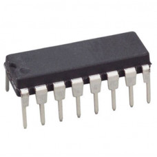
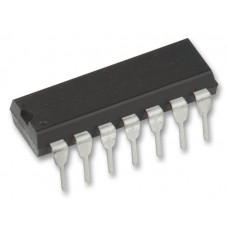
CD4015 Dual 4-Stage Shift Register IC DIP-16 Package
₹21.00
CD4015 consists of two identical, independent, 4-stage serial-input/parallel-output registers. Each register has independent CLOCK and RESET inputs as well as a single serial DATA input.
The CD4015-series types are supplied in 16-lead hermetic dual-in-line ceramic packages (F3A suffix), 16-lead dual-in-line plastic package (E suffix), 16-lead small-outline packages (M, M96, MT, and NSR suffixes), and 16-lead thin shrink small-outline packages (PW and PWR suffixes).
Features:-
- Medium speed operation…12 MHz (typ.) clock rate at VDD?? VSS?= 10 V
- Fully static operation
- 8 master-slave flip-flops plus input and output buffering
- 100% tested for quiescent current at 20 V
- 5-V, 10-V, and 15-V parametric ratings
- Standardized, symmetrical output characteristics
- Maximum input current of 1 ?A at 18 V over full package-temperature range; 100 nA at 18 V and 25?C
- Noise margin (full package-temperature range) =
- 1 V at VDD?= 5 V
- 2 V at VDD?= 10 V
- 2.5 V at VDD?= 15 V
- Meets all requirements of JEDEC Tentative Standard No. 13B, “Standard Specifications for Description of ?B? Series CMOS Devices”
- Applications:
- Serial-input/parallel-output data queueing
- Serial to parallel data conversion
- General-purpose register
Specifications:-
| Parameter | Specification |
| Part number | CD4015B |
| Technology Family | CD4000 |
| VCC (Min) (V) | 3 |
| VCC (Max) (V) | 18 |
| Voltage (Nom) (V) | 10 |
| F @ nom voltage (Max) (MHz) | 8 |
| ICC @ nom voltage (Max) (mA) | 0.3 |
| tpd @ nom Voltage (Max (ns) | 160 |
| IOL (Max) (mA) | 1.5 |
| IOH (Max) (mA) | -1.5 |
| 3-state output | No |
| Rating | See Data Sheet |
| Operating temperature range (C) | -55 to 125 |
Related Document:-
 ?CD4015 IC Datasheet
* Product Images are shown for illustrative purposes only and may differ from actual product.


MAECENAS IACULIS
Vestibulum curae torquent diam diam commodo parturient penatibus nunc dui adipiscing convallis bulum parturient suspendisse parturient a.Parturient in parturient scelerisque nibh lectus quam a natoque adipiscing a vestibulum hendrerit et pharetra fames nunc natoque dui.
ADIPISCING CONVALLIS BULUM
- Vestibulum penatibus nunc dui adipiscing convallis bulum parturient suspendisse.
- Abitur parturient praesent lectus quam a natoque adipiscing a vestibulum hendre.
- Diam parturient dictumst parturient scelerisque nibh lectus.
Scelerisque adipiscing bibendum sem vestibulum et in a a a purus lectus faucibus lobortis tincidunt purus lectus nisl class eros.Condimentum a et ullamcorper dictumst mus et tristique elementum nam inceptos hac parturient scelerisque vestibulum amet elit ut volutpat.


