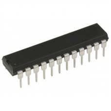
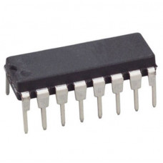
The CD4023 type is supplied in 14-lead hermetic dual-in-line ceramic packages (F3A suffix), 14-lead dual-in-line plastic packages (E suffix), 14-lead small-outline packages (M, MT, M96, and NSR suffixes), and 14-lead thin shrink small-outline packages (PWR suffix). The CD4023 type is also supplied in 14-lead thin shrink small-outline packages (PW suffix).
Features:-
- Propagation delay time = 60 ns (typ.) at CL?= 50 pF, VDD?= 10 V
- Buffered inputs and outputs
- Standardized symmetrical output characteristics
- Maximum input current of 1 ?A at 18 V over-full package temperature range; 100 nA at 18 V and 25?C
- 100% tested for quiescent current at 20 V
- 5-V, 10-V, and 15-V parametric ratings
- Noise margin (over full package temperature range:
1 V at VDD?= 5 V
2 V at VDD?= 10 V
2.5 at VDD?= 15 V - Meets all requirements of JEDEC Tentative Standard No. 13B, “Standard Specifications for Description of “B” Series CMOS Devices”.
Specifications:-
| Parameter | Specification |
| Part number | CD4023B |
| Technology Family | CD4000 |
| VCC (Min) (V) | 3 |
| VCC (Max) (V) | 18 |
| Channels (#) | 4 |
| Inputs per channel | 2 |
| IOL (Max) (mA) | 1.5 |
| IOH (Max) (mA) | -1.5 |
| Input type | Standard CMOS |
| Output type | Push-Pull |
| Features | Standard Speed (tpd > 50ns) |
| Rating | See Data Sheet |
| Data rate (Max) (Mbps) | 8 |
| Operating temperature range (C) | -55 to 125 |
| Package size: mm2:W x L (PKG) | 14PDIP: 181 mm2: 9.4 x 19.3 (PDIP|14) |
| Package Group | PDIP|14 |
Related Document:-
 ?CD4023 IC Datasheet
* Product Images are shown for illustrative purposes only and may differ from actual product.


