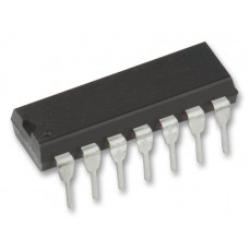
A high PRESET ENABLE signal allows information on the JAM INPUTS to preset the counter to any state asynchronously with the clock. A low on each JAM line, when the PRESET-ENABLE signal is high, resets the counter to its zero count. The counter is advanced one count at the positive transition of the clock when the CARRY-IN and PRE-SET ENABLE signals are low. Advancement is inhibited when the CARRY-IN or PRESET ENABLE signals are high. The CARRY-OUT signal is normally high and goes low when the counter reaches its maximum count in the UP mode or the minimum count in the DOWN mode provided the CARRY-IN signal is low. The CARRY-IN signal in the low state can thus be considered a CLOCK ENABLE.
The CARRY-IN terminal must be connected to VSS when not in use. Binary counting is accomplished when the BINARY/DECADE input is high; the counter counts in the decade mode when the BINARY/DECADE input is low. The counter counts up when the UP/DOWN input is high, and down when the UP/DOWN input is low. Multiple packages can be connected in either a parallel clocking or a ripple-clocking arrangement as shown in Figure 17. Parallel clocking provides synchronous control and hence faster response from all counting outputs. Ripple-clocking allows for longer clock input rise and fall times. The CD4029 is supplied in these 16-lead outline packages: Braze Seal DIP H4X Frit Seal DIP H1F Ceramic Flatpack H6W.
Features:-
? High-Voltage Type (20V Rating)
? Medium Speed Operation: 8MHz (Typ.) at CL = 50pF and VDD – VSS = 10V ? Multi-Package Parallel Clocking for Synchronous High Speed Output Response or Ripple Clocking for Slow Clock Input Rise and Fall Times
? ?Preset Enable? and Individual ?Jam? Inputs Provided ? Binary or Decade Up/Down Counting
? BCD Outputs in Decade Mode
? 100% Tested for Maximum Quiescent Current at 20V
? 5V, 10V and 15V Parametric Ratings
? Standardized Symmetrical Output Characteristics
? Maximum Input Current of 1?A at 18V Over Full Package-Temperature Range; 100nA at 18V and +25oC
? Noise Margin (Over Full Package Temperature Range): – 1V at VDD = 5V – 2V at VDD = 10V – 2.5V at VDD = 15V
? Meets All Requirements of JEDEC Tentative Standards No. 13B, ?Standard Specifications for Description of ?B? Series CMOS Device?s .
Specifications:-
| Parameter | Specification |
| Part number | CD4029BMS |
| DC Supply Voltage Range, (VDD) | ?-0.5V to +20V |
| Input Voltage Range, All Inputs | ?-0.5V to VDD +0.5V |
| DC Input Current, Any One Input | ?10mA |
| Operating Temperature Range | ?-55?C to +125?C |
| Storage Temperature Range (TSTG) | ?-65?C to +150?C |
| Lead Temperature (During Soldering) | ?+265?C |
(For more detailed specification refer Data Sheet)
Related Document:-
 ?CD4029 IC Datasheet
* Product Images are shown for illustrative purposes only and may differ from actual product.


