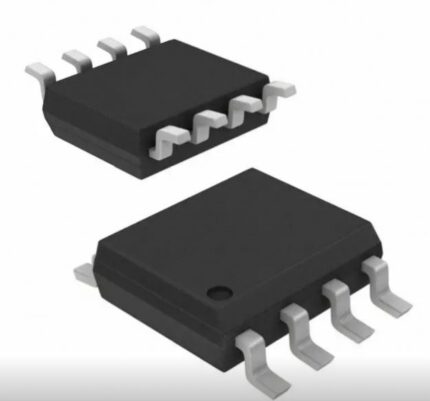
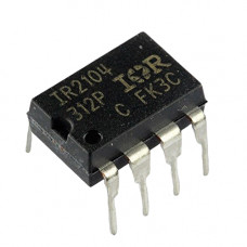
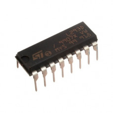
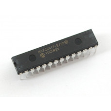
FAN7392 High and Low-Side Gate-Drive IC DIP-14 Package
₹120.00
The FAN7392 is a rnonolithic high- and low-sde gate drive IC that can drive high-speed MOSFETs and IGBTs that operate up to +600V. It has a buffered output stage with all NMOS transistors designed for high pulse current driving capability and minimum cross-conduction.
The FAN7392 is a rnonolithic high- and low-sde gate drive IC that can drive high-speed MOSFETs and IGBTs that operate up to +600V. It has a buffered output stage with all NMOS transistors designed for high pulse current driving capability and minimum cross-conduction. Fairch- ild’s high-voltage process and cornnwl-rnode noise can- celing techniques provide stable operation of the high- side driver under high dv/dt noise circumstances. An *Ivanced level-shift circuit offers high-side gate driver operation up to Vs=-9.8V (typical) for VBS=15V. Logic inputs are compatible with standard CMOS or LSTTL output. down to 3.3V logic The I-JVLO circuit prevents malfunction when VCC and VBS are lower than the speci- fied threshold voltage. The high-current and low-output vol* drop feature makes this device suitable for half- and full-bridge inverters, like power Sup- r DC-DC converter applications.
Features:-
Floating Channel for Bootstrap Operation to +600V
3AJ3A Sourcing/Sinking Current Driving Capability
Common-Mode dv/dt Noise Canceling Circuit
3.3V Logic Compatible Separate Logic Supply (VDD) Range from 3.3V to 20V
Under-Voltage Lockout for vcc and VBS Cycle-by-Cycle Edge-Triggered Shutdown Logic
Matched Propagation Delay for Both Channels
Outputs In-phase with Input Signals
Available in 14-DIP and 16-SOP (Wide) Packages
Specifications:-
Parameters Min Max Unit
High-Side Floating Supply Voltage-VB -0.3 625 V
High-Side Floating Offset Voltage-VS VB-25.0 VB+0.3 V
High-Side Floating Output VoltageVHO VS-0.3 VB+0.3 V
Low-Side Supply Voltage-VCC -0.3 25 V
Low-Side Floating Output Voltage-VLO -0.3 VCC+0.3 V
Logic Supply Voltage-VDD -0.3 VSS+25.0 V
Logic Supply Offset Voltage-VSS VCC-25.0 VCC+0.3 V
Logic Input Voltage (HIN, LIN and SD)VIN VSS-0.3 VDD+0.3 V
Related Document:-
FAN7392 IC Datasheet
* Product Images are shown for illustrative purposes only and may differ from actual product.


MAECENAS IACULIS
Vestibulum curae torquent diam diam commodo parturient penatibus nunc dui adipiscing convallis bulum parturient suspendisse parturient a.Parturient in parturient scelerisque nibh lectus quam a natoque adipiscing a vestibulum hendrerit et pharetra fames nunc natoque dui.
ADIPISCING CONVALLIS BULUM
- Vestibulum penatibus nunc dui adipiscing convallis bulum parturient suspendisse.
- Abitur parturient praesent lectus quam a natoque adipiscing a vestibulum hendre.
- Diam parturient dictumst parturient scelerisque nibh lectus.
Scelerisque adipiscing bibendum sem vestibulum et in a a a purus lectus faucibus lobortis tincidunt purus lectus nisl class eros.Condimentum a et ullamcorper dictumst mus et tristique elementum nam inceptos hac parturient scelerisque vestibulum amet elit ut volutpat.


