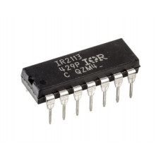
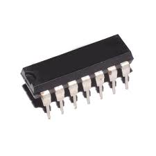
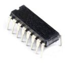
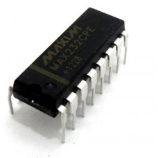
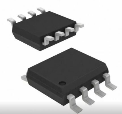
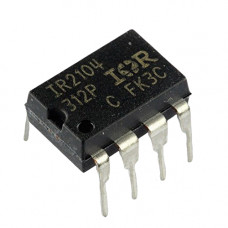
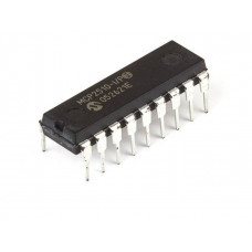
IR2113 High and Low Side Driver IC DIP-14 Package
₹175.00
IR2113 are high voltage, high speed power MOSFET and IGBT drivers with independent high and low side referenced output channels. Proprietary HVIC and latch immune CMOS technologies enable ruggedized monolithic construction.
- Part Number IR2113
- Manufacturer: Infineon Technologies
- Description: IC GATE DRVR HALF-BRIDGE 14DIP
- Detailed Description: Half-Bridge Gate Driver IC Non-Inverting 14-DIP
IR2113 are high voltage, high speed power MOSFET and IGBT drivers with independent high and low side referenced output channels. Proprietary HVIC and latch immune CMOS technologies enable ruggedized monolithic construction. Logic inputs are compatible with standard CMOS or LSTTL output, down to 3.3V logic. The output drivers feature a high pulse current buffer stage designed for minimum driver cross-conduction. Propagation delays are matched to simplify use in high frequency applications. The floating channel can be used to drive an N-channel power MOSFET or IGBT in the high side configuration which operates up to 500 or 600 volts.
Features of IR2113 Mosfet
- Floating channel designed for bootstrap operation Fully operational to 500V or 600V Tolerant to negative transient voltage dV/dt immune
- Gate drive supply range from 10 to 20V
- Undervoltage lockout for both channels
- 3.3V logic compatible Separate logic supply range from 3.3V to 20V Logic and power ground ?5V offset
- CMOS Schmitt-triggered inputs with pull-down
- Cycle by cycle edge-triggered shutdown logic
- Matched propagation delay for both channels
- Outputs in phase with inputs
Specifications of IR2113 Mosfet
- Parameter Min Max Unit
- VB-High side floating supply voltage -0.3 625 V
- VS- High side floating supply offset voltage VB -25 VB 0.3 V
- VHO- High side floating output voltage VS -0.3 VB 0.3 V
- VCC- Low side and logic fixed supply voltage -0.3 25 V
- VLO- Low side output voltage -0.3 VCC 0.3 V
- VDD- Logic Supply Voltage -0.3 VSS 25 V


MAECENAS IACULIS
Vestibulum curae torquent diam diam commodo parturient penatibus nunc dui adipiscing convallis bulum parturient suspendisse parturient a.Parturient in parturient scelerisque nibh lectus quam a natoque adipiscing a vestibulum hendrerit et pharetra fames nunc natoque dui.
ADIPISCING CONVALLIS BULUM
- Vestibulum penatibus nunc dui adipiscing convallis bulum parturient suspendisse.
- Abitur parturient praesent lectus quam a natoque adipiscing a vestibulum hendre.
- Diam parturient dictumst parturient scelerisque nibh lectus.
Scelerisque adipiscing bibendum sem vestibulum et in a a a purus lectus faucibus lobortis tincidunt purus lectus nisl class eros.Condimentum a et ullamcorper dictumst mus et tristique elementum nam inceptos hac parturient scelerisque vestibulum amet elit ut volutpat.
