
The memory devices (M29W800F and M29W400F) operate with VCC from 2.7V to 3.6V, offering access times of 55 ns or 70 ns. They feature fast programming times (10 µs per byte/word), multiple memory blocks including boot, parameter, and main blocks, and an embedded program/erase controller with suspend/resume modes. They support unlock bypass, temporary unprotection, and a common Flash interface with 64-bit security, ensuring low power consumption with standby options and up to 100,000 program/erase cycles per block.

Back to products

SM6T33A TVS Diodes 600W 33V
Original price was: ₹93.00.₹82.00Current price is: ₹82.00.
M29W800FB70N3F TR 3V, Parallel NOR Flash
₹224.00
NOR Flash 8Mb(x8/x16), 3V, Parallel NOR Flash, Bottom Boot, Automotive, 48TSOP, T&R
Description
Reviews (0)
Shipping & Delivery


MAECENAS IACULIS
Vestibulum curae torquent diam diam commodo parturient penatibus nunc dui adipiscing convallis bulum parturient suspendisse parturient a.Parturient in parturient scelerisque nibh lectus quam a natoque adipiscing a vestibulum hendrerit et pharetra fames nunc natoque dui.
ADIPISCING CONVALLIS BULUM
- Vestibulum penatibus nunc dui adipiscing convallis bulum parturient suspendisse.
- Abitur parturient praesent lectus quam a natoque adipiscing a vestibulum hendre.
- Diam parturient dictumst parturient scelerisque nibh lectus.
Scelerisque adipiscing bibendum sem vestibulum et in a a a purus lectus faucibus lobortis tincidunt purus lectus nisl class eros.Condimentum a et ullamcorper dictumst mus et tristique elementum nam inceptos hac parturient scelerisque vestibulum amet elit ut volutpat.
Related products

24LC256-I/SN
Features of? 24LC256-I/SN
? A single supply for use For? 24LC256-I/SN , it drops to 1.7V, whereas 24LC256 devices rise to 2.5V.
? CMOS Low-Power Technology:
Maximum write current is 3 mA. Maximum standby current is 1 A. (I-temp.)
? I2C Compatible, Two-Wire Serial Interface
? Up to eight devices can be cascaded
? Noise-cancelling Schmitt Trigger Inputs
? Ground Bounce is eliminated through output slope control.
? Compatibility with 100 kHz, 400 kHz, and 1 MHz
? Maximum Page Write Time: 5 ms
? Timed Erase/Write Cycle on Your Own
The 64-Byte Page Write Buffer
Equipment Write-Protect
? >4000V ESD Protection
? Over a Million Eraser/Writer Cycles
? >200 years for data retention
Factory programming is accessible for 24LC256-I/SN
24LC256-I/SN is RoHS conformant
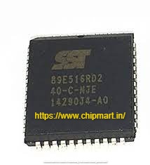
89E516RD2
The SST89E5xxRD2 and SST89V5xxRD2 are FlashFlex51 family 8-bit microcontroller devices designed and manufactured using SST's unique and proprietary Super Flash CMOS semiconductor manufacturing technology. SST's clients gain significantly from the split-gate device structure and thick-oxide tunnelling injector in terms of cost and reliability. The devices are pin-for-pin compatible with ordinary 8051 microcontroller devices and use the 8051 instruction set. The devices include 16/24/40/72 K Byte of on-chip flash EEPROM programme memory that is divided into two separate programme memory blocks. The primary Block 0 has 8/16/32/64K Bytes of internal programme memory space, whereas the secondary Block 1 has 8K Bytes of internal programme memory space.
The 8-KByte secondary block can be identified to the minimum address point in the 8/16/32/64 K Byte address space, as well as concealed from the programme counter and utilised as an independent EEPROM-like data store. In addition to the on-chip EEPROM programme memory of 16/24/40/72 K Bytes, the devices may address up to 64 K Bytes of external programme memory. In addition to 1024 x 8 bits of on-chip RAM, external RAM of up to 64 K Bytes may be addressed.
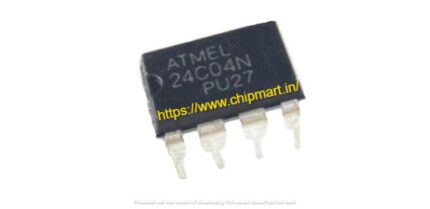
AT24CO4
Features
Low and Standard Voltage Operation: 2.7 (VCC = 2.7 to 5.5 V) and 1.8 (VCC = 1.8 to 5.5 V)
?128 x 8, 256 x 8, 512 x 8, 1024 x 8, or 2048 x 8 internal organisation (16K)
Bidirectional Data Transfer Protocol, Schmidt Trigger, Filtered Inputs for Noise Suppression, Two-wire Serial Interface, and Compatibility at 100 kHz (1.8V) and 400 kHz (2.7V, 5V)
8-byte page (1K, 2K), 16-byte page, Write Protect Pin for Hardware Data Protection (4K, 8K, 16K) Writing Styles
?High-reliability? Endurance: 1 Million Write Cycles? Data Retention: 100 Years ?Partial Page Writes Allowed ?Self-timed Write Cycle (5 ms max)
?Automotive Grade and Lead-free/Halogen-free Devices Available
?5-lead SOT23,8-lead TSSOP,8-lead PDIP,8-lead JEDEC SOIC,8-lead MAP, and 8-ball dBGA2 Packages
?Die Sales: Bumped Wafers, Waffle Packs, and Wafer Forms
The 1024/2048/4096/8192/16384 bits of serial electrically erasable and programmable read-only memory (EEPROM) provided by the AT24C01A/02/04/08A/16A are structured as 128/256/512/1024/2048 words of 8 bits each. The gadget is designed with a variety of industrial and business applications in mind, where low-power and low-voltage functioning are crucial. The AT24C01A/02/04/08A/16A is accessible through a Two-wire serial interface and is offered in compact 8-lead PDIP, 8-lead JEDEC SOIC, 8-lead MAP, 5-lead SOT23 (AT24C01A/AT24C02/AT24C04), 8-lead TSSOP, and 8-ball dBGA2 packages. There are other variants of the complete series in 2.7V (2.7V to 5.5V) and 1.8V (1.8V to 5.5V) voltage ranges.
AT25640B-SSHL-T
The Serial Electrically-Erasable Programmable Read-Only Memory (EEPROM) on the Atmel? AT25320B/640B has 32,768-/65,536-bits and is divided into 4,096/8,192 words with 8 bits each. The device is prepared for usage in a wide range of industrial and commercial settings where moderate and low-voltage functioning are critical requirements. The 8-lead JEDEC SOIC, 8-lead TSSOP, 8-lead UDFN, 8-lead XDFN, and 8-ball VFBGA packages for the AT25320B/640B are available in compact sizes. A 3-wire interface made up of Serial Data Input (SI), Serial Data Output (SO), and Serial Clock is used to access and enable the AT25320B/640B. (SCK). No further erase cycle is necessary before Write since every programming cycle is fully self-timed. Programming one of the four blocks of write security into the status register activates block write protection. For added data security, separate instructions for programme enable and programme disable are given. The WP pin offers hardware data protection to guard against unintentional write attempts to the status register. Any serial communication can be halted using the HOLD pin without having to restart the serial sequence.
HT9200A
The HT9200A/B tone generators are intended for use with C interfaces. aC can direct them to generate 16 dual tones and 8 single tones using the DTMF pin. The HT9200A has a serial mode, but the HT9200B has a selectable serial/parallel mode interface for a variety of applications such as surveillance systems, building automation, navigation system through telephone lines, communication systems, and so on.

M24128-DRDW8TP/K
Features? of M24128-DRD
- Support for all I2C bus modes? 1 MHz/ 400 kHz/ 100 kHz
- Memory bank- An EEPROM with 128 Kbits (16 Kbytes)
- Page Size in Bytes: 64
- In addition Make a locked page.
- Wider range of temperatures and voltages?40 to 105 degrees Celsius; 1.7 to 5.5 volts
- Schmitt trigger inputs are used to filter noise.
- Cycle time for short writes- Byte Write in 4 milliseconds- Page Write in 4 milliseconds
- Express cycling stamina. -4,000,000 Write Cycles at 25 ?C, - 1,2,000,000 Write cycles at 85 ?C & ? 900 k Cycles of writing at 105 ?C
- Data storage- at 105 ?C for more than 50 years., 200 yr at 55 ?C
- ESD Defense (Human Body Model)? 4000 V
- Packing is- Halogen-free and RoHS compliant
- SMD/SMT mounting style
- Case/Package: TSSOP-8
- Interface types: I2C and 2-Wire
- Size of Memory: 128 kbit
- Arrangement: 16 k x 8
- Minimum Supply Voltage: 1.7 V
- Maximum Supply Voltage: 5.5 V
- 40 C for the minimum operating temperature
- 105 C is the maximum operating temperature.
- 1 MHz is the maximum clock frequency.
- Time to Access: 450 ns
- Retention of Data: 200 Years
- Maximum Supply Current: 2 mA
- The M24128-DRD series
- mandatory requirement: AEC-Q100
- Packaging: Cut Tape and Reel
- Maximum Active Read Current: 2 mA
- STMicroelectronics is a brand.
- 2 mA is the operating supply current.
- Voltage Range for Operating Supply: 1.8 to 5.5 V
- Type of Product: EEPROM


M25P40-VMN6TPB
Features of M25P40-VMN6TPB?
- ?4 Mbit of Flash memory
- ?2.3 V to 3.6 V single supply voltage
- ?SPI bus compatible serial interface
- ?75 MHz clock rate (maximum)
- ?Page Program (up to 256 bytes) in 0.8 ms (typical)
- ?Sector Erase (512 Kbit) in 0.6 s (typical)
- ?Bulk Erase (4 Mbit) in 4.5 s (typical)
- ?Deep Power-down mode 1 ?A (typical)
- ?Hardware Write Protection: protected area size defined by three non-volatile bits (BP0, BP1 and BP2)
- ?Electronic signatures ? JEDEC standard two-byte signature (2013h) ? Unique ID code (UID) with 16 bytes read only, available upon customer request ? RES instruction, one-byte, signature (12h), for backward compatibility
- ?Packages ? RoHS compliant
- ?Automotive grade parts available
- Memory Size -
- Supply Voltage - Min: 2.3 V
- Supply Voltage - Max: 3.6 V
- Active Read Current - Max: 8 mA
- Interface Type: SPI
- Maximum Clock Frequency: 75 MHz
- Organisation: 512 k x 8
- Data Bus Width: 8 bit
- Timing Type: Synchronous
- Minimum Operating Temperature: - 40 C
- Maximum Operating Temperature: + 85 C
- Packaging: Reel / Cut Tape
- Memory Type: NOR
- Product Type: NOR Flash
- Speed: 75 MHz


W25Q16JV-SSIQ
Features of W25Q16JVSSIQ
- SpiFlash Memories' New Family - 16M-bit/ 2M-byte W25Q16JV - Common SPI: CLK, /CS, DI, and DO - CLK, /CS, IO0, IO1 and Dual SPI - CLK, /CS, IO0, IO1, IO2, IO3 for Quad SPI. - Hardware and Software Reset
- Best Serial Flash Performance - Single, Dual, and Quad SPI clocks at 133 MHz - Dual/Quad SPI equal to 266/532MHz - Continuous data transfer rate of 66 MB/S - No fewer than 100K Program-Erase cycles per sector - Retention of data for more than 20 years
- A productive "Continuous Read" - Constant Read with 8/16/32/64-Byte Wrap - Address memory with as few as 8 clocks - Facilitates real XIP (execute in place) operation - Performs better than X16 Parallel Flash
- Wide temperature range, low power - Single 2.7 to 3.6 volt supply - Operating range: -40 to +85 ?C. - Operating temperature range: -40 to +105 ?C. - Power-down, 1A.
- 4KB sectors and flexible architecture - 4K/32K/64K-Byte Uniform Sector/Block Erase - Programmable pages can hold up to 256 bytes. - Delete/Suspend/Resume Program
- Features of Advanced Security - Write-Protect in Software and Hardware - Lock-Down Power Supply and - Extraordinary OTP security - Protection for the top/bottom and complement arrays - Protection for individual blocks and sectors - Each device has a 64-Bit unique ID. - Register for Discoverable Parameters (SFDP) - OTP locks on 3X256-Byte Security Registers - Bits in the Volatile & Non-Volatile Status Register
- Effective Packaging for Space - 8-pin SOIC 150/208 mils - USON 8-pad 2X3mm/4X3mm - XSON 8-pad 4x4-mm - WSON 8-pad 6x5-mm ? 8-ball WLCSP - For KGD and additional alternatives, contact Winbond


Reviews
There are no reviews yet.