Description of? SN74LVCH8T245
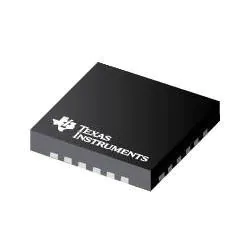
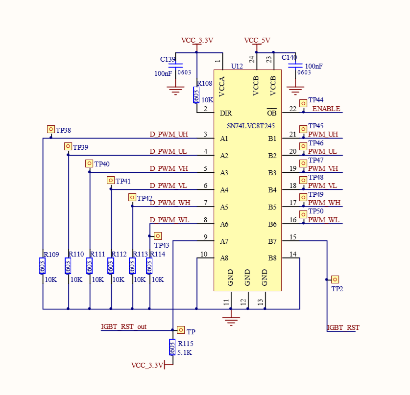
A bidirectional voltage level translator with customizable dual power supply rails, the SN74LVC8T245 is an eight bit non-inverting bus transceiver. The VCCA and VCCB settings for the SN74LVC8T245 are designed to function between 1.65 V and 5.5 V.
The A port’s purpose is to monitor VCCA. Any supply voltage between 1.65 V and 5.5 V is accepted by VCCA. VCCB tracking is intended for the B port. Any source voltage between 1.65 V and 5.5 V is accepted by VCCB. The 1.8-V, 2.5-V, 3.3-V, and 5.5-V voltage nodes can all be translated in either direction at low voltage thanks to this.
For asynchronous communication between two data buses, the SN74LVCH8T245 is intended. The direction-control (DIR) input and output-enable (OE) input’s logic levels can either activate the B-port outputs or the A-port outputs, or they can both be put into a high-impedance state.
When the B-port outputs are turned on, the device transmits data from the A bus to the B bus, and when the A-port outputs are turned on, it transmits data from the B bus to the A bus. Both the A and B ports’ input circuitry is constantly active.
Active bus-hold circuitry maintains the logic state of idle or undriven inputs. It is not advised to use pullup or pulldown resistors with the bus-hold circuitry. This device meets the requirements for Ioff applications involving partial power reduction.
The Ioff circuitry turns off the outputs to stop harmful current from flowing back into the device. The VCC isolation feature makes sure that the outputs are in the high-impedance condition if either VCCA or VCCB is at GND.
OE should be connected to VCCA through a pullup resistor to assure the high-impedance state during power-up or power-down; the minimum value of the resistor is dictated by the driver’s capacity to sink current. The control pins (DIR and OE) of the SN74LVCH8T245 are intended to correspond to VCCA.




Reviews
There are no reviews yet.